Capabilities

Altaflex continues to invest in technology to support new and existing customers with global interconnect solutions. Our goal is to empower customers by providing a toolbox of technologies and capabilities to help develop tomorrow’s products.
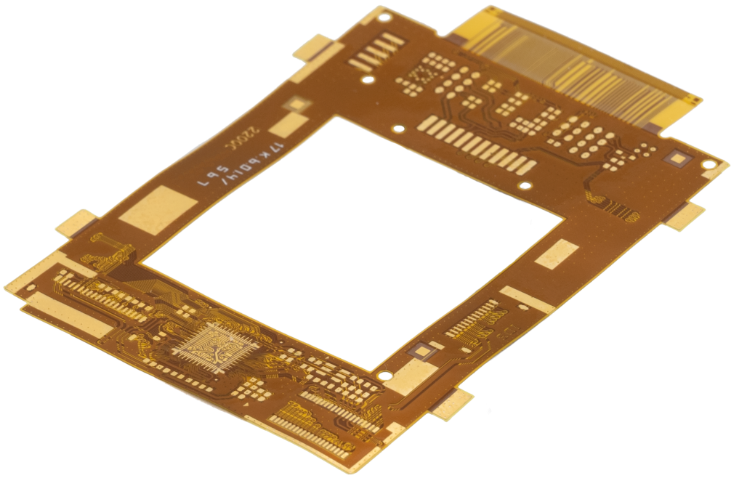
Laser Direct Imaging

10 μm feature size

Drilling

UV Yag Laser systems

20 μm beam width for high accuracy

High-speed NC drill

vision alignment/scaling

Inspection

Automated Optical Inspection down to 8 μm feature size

X-Ray inspection for via alignment and solder paste

X-Ray Fluorescence measurement of surface finish thicknesses

Inkjet legend printing

Provides fully customizable serialization and date coding

Testing

Flying probe electrical tester

Micro needle probes for minimal witness mark

Smallest pad size: 35 μm, 100 μm pitch.

Impedance testing at 20GHz

short-trace measurements down to 0.75 inches

On-part measurements

Feature
High Density
Standard
Minimum Copper Trace/Space
0.25 oz. (9 μm)
0.001"/0.0015"
25 μm/38 μm
0.0015"/0.002"
38 μm/50 μm
0.33 oz. (12 μm)
0.0015"/0.0015”
38 μm/38 μm
0.002"/0.002"
50 μm/50 μm
0.5 oz. (18 μm)
0.002"/0.002"
50 μm/50 μm
0.0025"/0.0025”
64 μm/64 μm
1 oz. (35 μm)
0.003"/0.003"
75 μm/75 μm
0.0035"/0.0035’
89 μm/89 μm
Minimum Via Hole Diameter
NC Drill
0.003"
75 μm
0.006"
150 μm
UV Laser
0.002"
50 μm
0.004"
100 μm
Minimum Blind Via Diameter
UV Laser
0.004"
100 μm
0.006"
150 μm
Layer to Layer Artwork Registration
Double Sided
0.001”
25 μm
0.004”
100 μm
Trace to Edge Tolerance
NC Route
NA
NA
0.005"
125 μm
UV Laser
0.001"
25 μm
0.001"
25 μm
Insulator Positional Tolerance
Cover Film
0.001”
25 μm
0.003"
75 μm
LPI
0.001”
25 μm
0.002"
50 μm
Minimum Cover Layer Opening
0.5 mil (12 μm)
0.0005”
12 μm
0.001”
25 μm
1 mil (25 μm)
0.001”
25 μm
0.002"
50 μm
Cover Layer Adhesive Bleed
0.5 mil (12 μm)
0.0005”
12 μm
0.001”
25 μm
1 mil (25 μm)
0.001"
25 μm
0.002"
50 μm
Minimum Cover Layer Webbing Width
0.5 mil (12 μm)
0.004”
100 μm
0.004”
100 μm
1 mil (25 μm)
0.006"
150 μm
0.006"
150 μm